Thin film DMDs
We can make reflective light spatial modulators thanks to micro mirror matrices, using actuators made of micro-machined piezoelectric film to control the slew angle of each matrix micro mirror in order to define the gray-scale of each pixel in the screen. The reflected light on a mirror surface makes a rectangular shaped image on the projection shutdown screen, which moves along the horizontal axis as the slew angle is changing. When a micro mirror doesn't swivel, all the reflected light is stopped and adsorbed on the shutdown screen and the pixel image on the screen is off. When the micro mirror has swiveled at full capacity, all the reflected light goes through the shutdown screen, the pixel image on the screen is on. The quantity of light going through the shutdown screen is proportional to the tilt angle of each mirror. A specific control of slew angles allows to create grey levels on the screen between the extreme brightness states (on-off). Therefore, thin film micro mirror systems share the functional necessity to create matrices with a DMD system, on which they add the necessity of the nanoscale control of the precision positioning for gray-scales
Each pixel consists of a bilayer structure: a mirror and an actuator layer. The mirror rotation is ensured by a piezoelectric thin film actuator in the form of clamped micro beam. As you see in the photograph below, a mirror is connected to the lower clamped micro beam thanks to a suspension arm.

The beams are tied to the PMOS substrate. Each clamped beam consists of a non-stoichiometric silicon (SiNx) nitride layer, which is used as a support for a platinum inferior electrode, a piezoelectric layer and a platinum superior electrode. When there is voltage between the two electrodes, the piezoelectric layer contracts in the horizontal direction and dilates in the vertical one. As a result, the beam neutral line moves forward the inferior electrode due to the layer of the thickness of the basis layer, and the mechanical contraction of the piezoelectric layer produces a vertical refraction of the beam upwards and as a consequence, the inclination of the mirror on it.
Thin film micro mirror matrix devices are made in one block on active PMOS matrix through surface micro-machining techniques. The active matrix is a transistor network sending a video signal to each pixel. The size of each mirror is 49 µm x 49 µm for XGA systems.
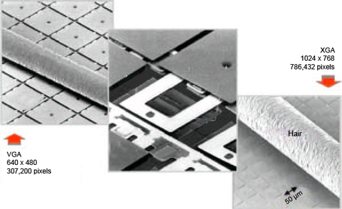
The aluminum is sprayed on the upper sacrificial layer of mirror layers. Aluminum layer is micro-machined with dry etching to shape mirrors. Sacrificial layers are put off to make the needed air gaps. As we must use two different materials for these layers, the crowning process has two steps. First, the superior sacrificial layer is cleared through the gaps between reactive ion etching mirrors. Then, the complete crowning of this layer is done, and the sacrificial layer is exposed to the air and is eliminated by a xenon fluoride vapor etching. These two techniques have high lateral etching speeds, don't produce any residue, don't etch nor damage the other layers. The picture above deals with electronic microscope snapshots completed by VGA and XGA matrix after the sacrificial layers release process. The 800 000 final mirrors of t XGA device show initial inclination positions of 0° ± 0.03°.
A 5 400 lumen operational projector prototype with 3 thin film micro mirror matrix systems and a 1 kW xenon lamp was presented during the 1998 Asian Display Fair, and offered a light transmission overall efficiency of 22%.
The clamped piezoelectric micro beam actuators of thin film micro mirror matrices were used not only for the display but also for the quick scanning of AFM probe matrices and the adaptation of mechanical constraints in photonic devices.