Infrared non-cooled bolometers
Infrared sensors allow to identify and represent objects according to their emission temperature. Thanks to thermal imaging we can measure the temperature at a distance and have the possibility to see in the dark, in smoke and when the weather is very cloudy. Until a few times ago, high performance IR cameras required very expensive systems without cooling that went until cryogenic temperatures to detect photons and eliminate thermal noise. More recently, sensor working at room temperature has been developed using micro machined bolometers and pyroelectric detectors. FPA (Focal Plane Array) infrared structures can produce infrared images or objects for sets made by human beings transforming the led temperature changes into electrical signals. Non-cooled bolometers use the led changes by temperature in electrical resistance, polarization and dielectric properties of the material composing detectors.
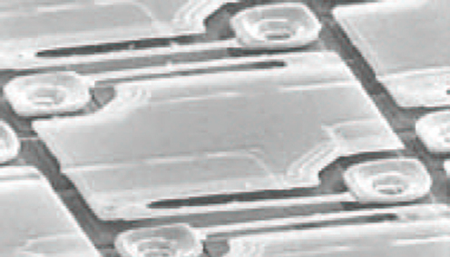
These detectors need a high thermal insulation with the substrate to get a high sensitiveness. Micro technologies play an important part in the manufacture of such weak specific heat capacity detectors with a thermal insulation exceptionally high. Honeywell is marketing a resistive bolometer 2D matrix with an insulating structure (see picture below).
![[zoom...]](javascript:window.open(%22../res/fig_05_1.jpg%22,%22_blank%22,%22width=%22+Math.min(800,screen.availWidth)+%22,height=%22+Math.min(600,screen.availWidth)+%22,left=%22+(screen.availWidth-800)/2+%22,top=%22+(screen.availHeight-600)/2+%22,scrollbars=yes,resizable=yes%22)?void(0):void(0))
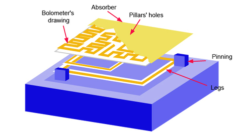
The nitride silicon membrane is suspended by two arms above the silicon substrate. The size of the suspension arm is calibrated in order to have a thermal conductivity of 8x10⁻⁸ W/°K. The plate specific heat capacity is 8x10⁻¹⁰ J/°K and the response time in temperature is 10ms. Working at a pace of 30 frames per second with a f/1 optics, the NETD (Noise Equivalent Temperature Difference) has been measured at 0.04°C with vanadium oxide resistance. Another alternative consists in developing a 2D monolithic matrix by using the pyroelectric properties of lead titanate with an insulation system similar to the one developed by Honeywell. The NETD announced for this device was 0.01°C and was adopted for several similar applications.
On the photo below, you can see a three level device manufactured by Kim and his team.
![[zoom...]](javascript:window.open(%22../res/fig_06_1.jpg%22,%22_blank%22,%22width=%22+Math.min(800,screen.availWidth)+%22,height=%22+Math.min(600,screen.availWidth)+%22,left=%22+(screen.availWidth-800)/2+%22,top=%22+(screen.availHeight-600)/2+%22,scrollbars=yes,resizable=yes%22)?void(0):void(0))
The main goals of this device were to increase the filling factor (92% against 62% for the Honeywell device) and to minimize thermal conductivity, similar to that of the Honeywell planar device.