Digital Recording
Firstly, let's concern ourselves with the discretisation effect of the pixelated recording material. As we have already mentioned, digital holography dates form the 1970s and became more seriously accessible from the beginning of the 1990s.
The main advantage of digital photosensitive material is that the image is acquired quickly without having the chemical development stage, which represents a considerable time gain. Another advantage is that these plates are reusable once the data is stored.
The image sensor is now replacing the analogue photosensitive plate. The process for a recording a digital hologram is similar to that used in classic holography, in that the object diffracts a wave which interferes with the reference wave in the recording plane.
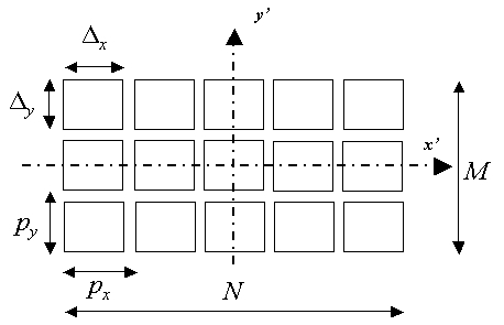
However, the spatial discretisation of the recorded pattern and the dimensions of the pixel elements impose certain conditions on the recording of a hologram. It is considered that the recording plate is a pixel matrix. The recording of a hologram on a digital photo plate not only discretises the photo plane but also integrates the temporal and spatial flux onto it. Whatever technology is used, the digital recording will (depending on the directions x' and y' on the recording plane) consist of,
 pixels at a pitch of
 . Each of these pixels is of a dimension
 .
.
Figure 11 depicts the pixel matrix.

As far as sensor technology is concerned, we mainly talk about CCD (charge-coupled device) sensors and CMOS (complementary metal-oxide-semiconductor) sensors. Matrices made up of photosensitive elements called pixels are generally square-shaped. Their size varies from
 to
to
 . Thus, the spatial resolution of such sensors is between
 and
and
 , values which should be compared with those given in table 1 for so-called “analogue” recording materials.
Pixelised sensors offer by far the worst spatial resolution for the recording of holograms. The way these devices work is based on the photoelectric effect which causes the conversion of incident photons into electrons with a quantum efficiency of
 . Silicon is the main element among the photosensitive elements. The sensor encodes the image using between 8 and 16 bits and each pixel contains
 electrons at saturation point. The value of
 is several tens of thousands of electrons, typically between 10,000 and 40,000. the average sensitivity of these sensors can be evaluated for comparison purposes with the values given in table 1.
As the pixels have a surface area of
 , the average necessary exposure needed to fill half the quantum well, is given by :
Where
 is the Planck constant and
 is the speed of light in the vacuum.
A digital device with
 ,
,
 ,
,
 and
and
 gives
gives
 . Silicon-based matrix sensors are therefore on average more than ten times more sensitive than the photosensitive plates listed in table 1.
Given the spatial extension of the pixels, the hologram at a certain coordinates
 can be written :
With the pixel function :
The pixel function is even. The pattern of interferences recorded by a pixel at the coordinates
 is mathematically represented by a convolution product of the analogue hologram by the pixel function :
The digital hologram recorded as an image is a juxtaposition, depending on the two dimensions, of all the integration surfaces. This image is mathematically represented by the following relationship :
The pixel function therefore has a smoothing effect which is to say of by low pass filtering over the raw hologram.
Thus, the recording of a digital hologram can be classified as a “low resolution” recording while recording using the “analogue” silver photo plates are classed as “high resolution”.