PN junction under reverse bias
Under reverse bias (V<0), whatever the weak voltage applied to the junction, the total current is fixed to -Js. This current is called the saturation current. However, for high reverse voltages, the reverse current can suddenly increase. It is then possible to reach the breakdown voltage of the junction, denoted Vc. Indeed, when the reverse voltage is increased, the electric field is increased accordingly inside the junction. But the electric field cannot exceed a given value
 . This is because as the electric field increases, so does the electrostatic force
 acting on the electrons linked to the crystalline network; this force can at some point become so high that it exceeds the binding force linking the valence electrons to their respective nuclei. As these electrons are released, the crystal becomes conductive and neither the electric field nor the voltage can increase any more. This means that the maximum electric field that can be applied to a semiconductor crystal is the field that would lead to the direct excitation of an electron from the valence band to the conduction band, or stated differently the field leading to the material ionization.
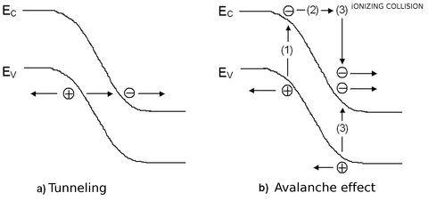
This breakdown effect can be related to two different physical phenomena. The first one is a tunneling effect called the Zener effect. The presence of a high electric field (~106V/cm for silicon) creates electron-hole pairs. The electrons associated to these pairs are emitted through the depletion zone, from the valence band to the conduction band, without loss or gain in energy, hence the term of tunneling used for this effect. In practice, one may observe the Zener effect only for highly-doped PN junctions, in which the space charge zone is narrow
 so that the “tunnel” is short enough to be crossed.
When the depletion region is not so narrow, typically for
 , another phenomenon called the avalanche breakdown effect arises and provokes the junction breakdown well before the Zener effect can be observed. For electric fields of the order of 105V/cm, which is about 10 times smaller than the threshold for the Zener effect, the acceleration of some carriers is sufficient to enable the generation of electron-hole pairs by collisions with the atoms of the crystal network. These pairs are then accelerated and provoke the creation of other pairs. The result is a chain reaction creating an avalanche effect. This process is illustrated in figure EC7. It can be described as follows: phase (1) corresponds to the thermal generation of an electron-hole pair ; during phase (2) the electron is accelerated by the electic field and is subsequently promoted to a higher lying level within the conduction band, where it is referred to as a “hot carrier”; in phase (3) the electron kinetic energy is high enough to create another electron-hole pair thanks to collisions: after the impact, called the ionization impact, the electron having lost its energy is brought back to the bottom of the conduction band while a second electron-hole pair is created. If the thickness of the depletion band is large enough the process can repeat itself. The process described here for electrons can also occur with holes.
