Doped (extrinsic) semiconductors
An extrinsic semiconductor is a semiconductor doped by a specific impurity which is able to deeply modify its electrical properties, making it suitable for electronic applications (diodes, transistors, etc.) or optoelectronic applications (light emitters and detectors).
P-type semiconductors
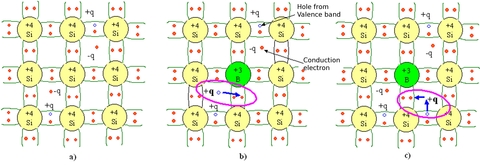
A P-type semiconductor is an intrinsic semiconductor (like Si) in which an impurity acting as an acceptor (like e.g. boron B in Si) has been intentionally added. These impurities are called acceptors since once they are inserted in the crystalline lattice, they lack one or several electrons to realize a full bonding with the rest of the crystal.
![[zoom...]](javascript:window.open(%22../res/c_fig_05_1.jpg%22,%22_blank%22,%22width=%22+Math.min(800,screen.availWidth)+%22,height=%22+Math.min(600,screen.availWidth)+%22,left=%22+(screen.availWidth-800)/2+%22,top=%22+(screen.availHeight-600)/2+%22,scrollbars=yes,resizable=yes%22)?void(0):void(0))
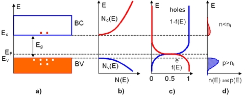
From figure 5, we see that a p-type semiconductor has a lower electron density n and a higher hole density p than the same intrinsic semiconductor. Electrons are said to be the minority carriers whereas holes are the majority carriers.
For extrinsic semiconductors, the dopant density is always far higher than the intrinsic carrier density : NA>>ni. In the case of a p-type material, the hole density is then close to the dopant density NA. Since the law of mass action is always true, we obtain the following expressions for the carrier densities
The Fermi level for a p-type semiconductor or chemical potential is then :
When the acceptor density is increased, the Fermi level moves closer to the edge of the valence band. If NA=Nv the Fermi level enters the valence band, the semiconductor is then said to be degenerate.
The important points regarding p-type semiconductors are summarized graphically in figure 6.
![[zoom...]](javascript:window.open(%22../res/c_fig_06_1.jpg%22,%22_blank%22,%22width=%22+Math.min(800,screen.availWidth)+%22,height=%22+Math.min(600,screen.availWidth)+%22,left=%22+(screen.availWidth-800)/2+%22,top=%22+(screen.availHeight-600)/2+%22,scrollbars=yes,resizable=yes%22)?void(0):void(0))
N-type semiconductors
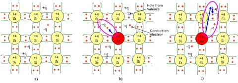
A N-type semiconductor is an intrinsic semiconductor (e.g. silicon Si) in which a donor impurity (e.g. arsenic As in Si, or Si in GaAs) has been intentionally introduced. The impurities are called donor impurities since they have to give an extra electron to the conduction band in order to make all the bonds with neighboring atoms (As is pentavalent while Si is tetravalent).
![[zoom...]](javascript:window.open(%22../res/c_fig_07_1.jpg%22,%22_blank%22,%22width=%22+Math.min(800,screen.availWidth)+%22,height=%22+Math.min(600,screen.availWidth)+%22,left=%22+(screen.availWidth-800)/2+%22,top=%22+(screen.availHeight-600)/2+%22,scrollbars=yes,resizable=yes%22)?void(0):void(0))
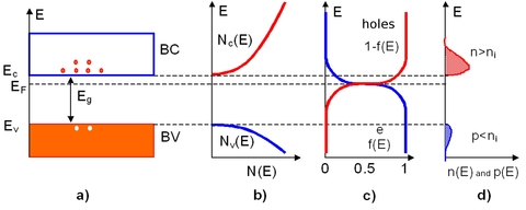
From figure 7, we see that a n-type semiconductor has a higher electron density n and a lower hole density p than the same intrinsic semiconductor. Holes are said to be the minority carriers whereas electrons are the majority carriers.
Like in p-type semiconductors, we can write the following relationships, where ND is the donor density :
The Fermi level for a n-type semiconductor is then :
When the donor density is increased, the Fermi level moves closer to the edge of the conduction band. If ND=Nc the Fermi level enters the conduction band, the semiconductor is then said to be degenerate.
The important points regarding n-type semiconductors are summarized graphically in figure 8.
![[zoom...]](javascript:window.open(%22../res/c_fig_08_1.jpg%22,%22_blank%22,%22width=%22+Math.min(800,screen.availWidth)+%22,height=%22+Math.min(600,screen.availWidth)+%22,left=%22+(screen.availWidth-800)/2+%22,top=%22+(screen.availHeight-600)/2+%22,scrollbars=yes,resizable=yes%22)?void(0):void(0))