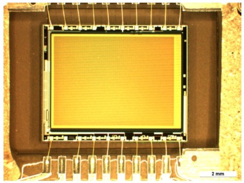
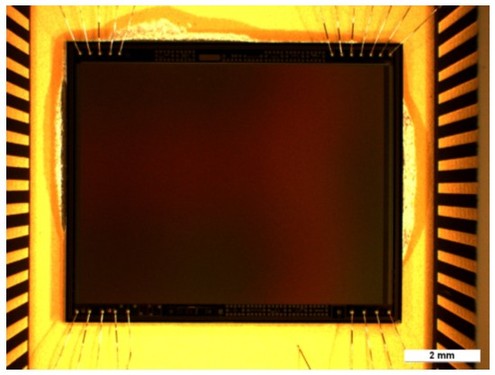
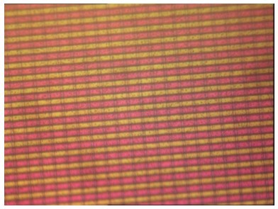
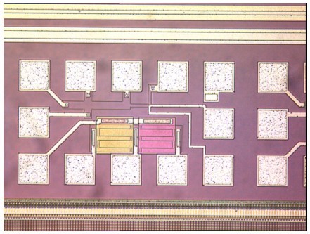
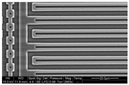
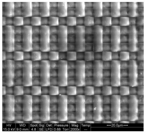
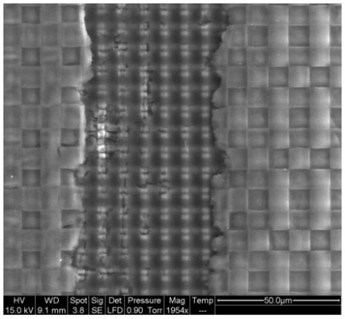
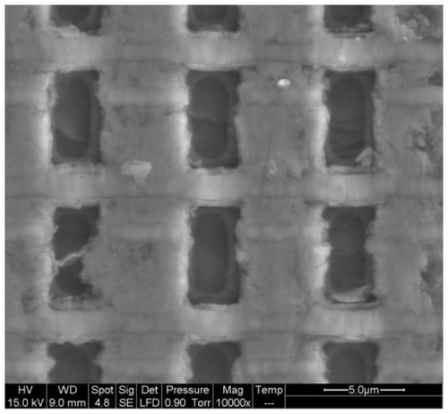
These photographs were taken after complete disassembly (including glass shield) of an interline transfer color sensor (Sony) and a frame transfer sensor (Kodak). The photographs were taken with a binocular loupe and an optical microscope both equipped with a system of image acquisition. Other images were also taken with a Scanning Electron Microscope, but the presence of some varnish or glass film of protection did not allow to go deeper into the sensors... We present them as purely illustrative.
Figure 43: Full field view of a Sony sensor (photo EMA)
[zoom...]Info
Figure 44: Full field view of a Kodak sensor (photo EMA)
[zoom...]Info
Figure 45: Pixels of a Kodak Megaplus 1.4 (400x) (photo EMA)
[zoom...]Info
Figure 46: Output register and drains of the Kodak Megaplus 1.4 (200x) (photo EMA)
[zoom...]Info
Figure 47: Output register and drains of the Kodak Megaplus 1.4 (MEBE) (photo EMA)
[zoom...]Info
Figure 48: Manufacturing markers of the Kodak Megaplus 1.4 (200x) (photo EMA)
[zoom...]Info
Figure 49: Photosites for calibration of the Kodak Megaplus 1.4 (200x) (photo EMA)
[zoom...]Info
Figure 50: Output register of the Kodak (MEBE) (photo EMA)
[zoom...]Info
Figure 51: Microlenses on a SONY sensor (photo EMA)
[zoom...]Info
Figure 52: Sony sensor after scratching off of the microlenses (photo EMA)
[zoom...]Info
Figure 53: Pixels of the Sony sensor (after scratching off of the microlentses) (photo EMA)
[zoom...]Info
Figure 54: Pixel the SONY sensor (after scratching off of the microlentses) (photo EMA)
[zoom...]Info
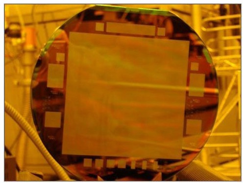
Figure 55: 110 Mpixels sensor, of 4 inches², 10560*10560 pixels, (photo Dalsa)
[zoom...]Info
Figure 56: Commercial large format CCD sensors
[zoom...]Info

