CMOS sensors
CMOS sensors were created at the beginning of the 1990s.
Among other things, they can directly make the charge conversion on the generation photosite thanks to their pixel amplifier. This characteristic give them the ability to get rid of several transfers and to increase the processing speed. Their main advantages come from the way they are manufactured.
-
Manufacturing identical (90%) to computer chips (particularly to the DRAM Dynamical Random Access Memory),
-
Cheap mass-production,
-
Direct charge conversion without any transfer: neither blooming nor smearing,
-
Each pixel has its own amplifier, no shift register: Active Pixel Sensor,
-
Each pixel can be individually addressed,
-
No complex time clocks,
-
Low energy consumption (100 times less than CCD),
-
High reading rate.
In the last few years, they have really come to the fore compared to the CCD sensors, which is directly linked to them being used in cellular telephony as video devices or on-board cameras. This is a direct consequence of their low-cost manufacturing and low consumption.
For scientific applications, it is their operating speed (image rate), linked to the charge conversion on the creation site, which make them more appropriate for used than the CCDs. One of the last generation sensors can digitize 1024 x 1024 pixel images to a 5400 images/second rate...
More over, each pixel can be independently driven (manually or automatically), which explains that they can be used in vision for highly contrasted scenes. However, they do induce a slight bias, which can generate major differences between the images sensed by the human eye and the rough image coming from the CMOS sensor.

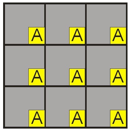
The size of the sensors is similar to the CCD's nd can be close to a micrometer in some cases. One of the problems raised by the CMOS technology is the loss in spatial resolution due to the presence of the amplifier A on the photosite (comparable to the optic nerve on the human retina). This is shown on figure 32 (sensitive surface in grey and amplifier in yellow). At first, only one transistor was used to amplify. Nowadays, these amplifiers can include 3 to 5 transistors (3T and 5T CMOS) and the fill factor can be significantly diminished.

However, this loss can be compensated by using micro lenses, like for CCD with line transfer. Moreover, the fill factor is always higher for Full Frame CCD than for 3T CMOS sensors. For some CMOS models, we can also notice that even if the amount of information transferred is high, the performances in terms of signal-to-noise ratio can be inferior to the CCD's.
However, they are more and more used in digital photography and lots of manufacturers include them in their digital box. Since 2007, CMOS sensors of more than 12.4 effective megapixels have allowed users to come close AND TO EXCEED the 24 x 36mm size, usually associated to photography. Since more recent days, CMOS are usually linked to an analog-to-digital converter by column, which improves the data acquisition speed up to almost 10 images/second.
Finally, there is a tendency to develop smart cameras, in which thanks to the CMOS high-speed transfer associated with on-board processing, an interpreted image can be directly downloaded at the exit. Some of the smart camera functions are then directly integrated into the chip. This operating mode has more advantages in terms of size and simplicity. Figure 33 shows the comparative schematic drawing of all the ways that can result in data acquisition.

Nowadays, CCD and CMOS cost pretty much the same for similar quantities (high-quality CMOS are manufactured on assembly lines separate from the DRAM...). For performant applications, the final decision does not have anything to do with “CCD or CMOS” but takes into account the adequacy of the product with the task that needs to be carried out.
We need to keep in mind that CMOS allow high speed but that CCD keep on being the best for their high dynamics and their better fill factor.